Motivation
- Good signal integrity (lots of decouple caps), good OSC (the one you choose)
- Shielded!
- inlcude your favorite DCDC, flexibility (no additional space for that)
- Solder @Home (Reflow or by hand, footprints as big as possible)
- Breadboard compatible, 2.54mm Pinheader
- Antenne pad with option for RP-SMA
- Availability of many GPIOs
- Opensource
Specification
- 2 PCBs with 2 Layers each. ESP8266 in between
- 1. PCB: with ESP8266
- 2. PCB: above ESP8266, acting as shield and for placement of DCDC
- Alltogether 4 Layers
- Allignment of PCBs via Pinheader (holes in both PCBs)
- DCDC of your choice on 2. PCB. Maybe also small uC, USB
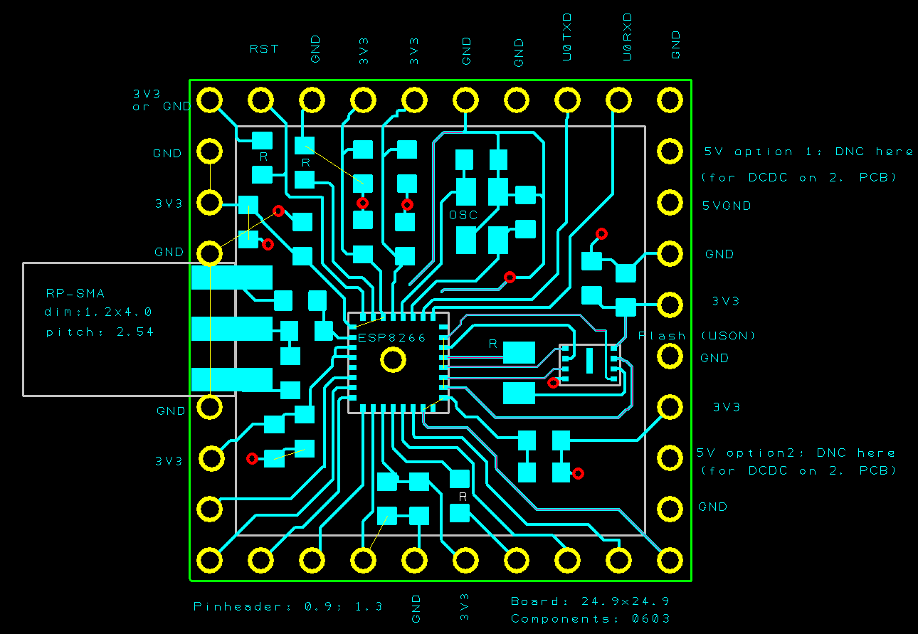
- Using multiple VCC3V3-Pins of pinheader on 1. PCB (see image)
Layout description
- Side view: see attachment
- 1. PCB Layer 1: Signals, ESP8266, C, R (see attachment)
- 1. PCB Layer 2: Ground
- 2. PCB Layer 1: DCDC, custom components
- 2. PCB Layer 2: Combine 3V3, Ground
- Customizing the 2. PCB is easy
Cost of materials
- Make 4 PCBs on 5x5cm (your favorite PCB manufacture)
- I estimated 8USD (including RP-SMA, DCDC, both PCBs, 10ppm-OSC, a.s.o.). One can do better.
Ideas for placing
- under ESP8266: no solder mask, no cooper
- Surround ESP8266 with solder mask, traces to the edge of the package
- Via under ESP8266. Make the via rest-ring plane; solder this subsequently
- Placing USON Flash: Todo; Alternative: bigger package on 2. PCB
Considerations for solder
- Use low-temperature solder. Do not overheat 0.6mm-PCB.
50Ohm considerations
- Thickness of 1. PCB: 0.6mm. -> 50Ohm trace: approx. 1mm
- Witdh of RP-SMA pad: approx. 1mm
- Width of 0603 footprint: approx 1mm
Where is the Opensouce layout?
There is quite some work in making this concept and in doining such a placing. If you would like to continue from here on, you are very welcome. Otherwise, I will make and provide the layout in approx. 3 month. Bussy at the moment.
Note: Design is based on documentation that is or was freely available.
Edit: Changed note.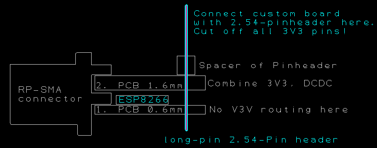
Statistics: Posted by Lars R. — Fri Oct 31, 2014 10:00 pm
]]>